PCB overmolding not only shields the PCB from external threats (such as moisture, temperature variations, and mechanical stress) but also enhances the overall appearance and functionality of the device. In this comprehensive guide, we will explore the world of PCB overmolding, delving into its benefits, applications, materials, and best practices. Whether you’re a manufacturer looking to enhance your plastic bonding product durability or an engineer seeking to optimize your PCB design for overmolding, this guide will provide you with the insights and knowledge you need to make informed decisions.
What is PCB Overmolding?
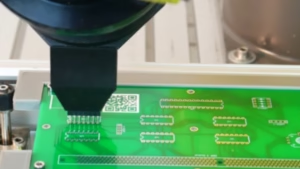
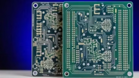
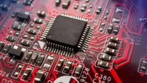
PCB overmolding is a specialized manufacturing process of applying a molded plastic layer over a PCB, creating a robust and sealed assembly. This protective layer serves as a barrier against various environmental factors such as moisture, dust, and mechanical stress, which can potentially damage the sensitive electronic components on the PCB. By providing this encapsulation, overmolding significantly improves the longevity and performance of electronic devices.
PCB Overmolding Process
Preparation of the PCB:
The first step involves preparing the PCB assembly (PCBA) by ensuring that it is clean and free of contaminants. Sensitive components may be pre-encapsulated to protect them from mechanical stress and temperature variations during the overmolding process.
Material Selection:
Choosing the right overmolding material is crucial. Common materials include thermoplastics and thermosets, which must be compatible with the PCB components to avoid any adverse chemical reactions. The selected material should also provide the necessary mechanical and thermal properties to withstand the intended application.
Injection Molding:
The overmolding material is heated until it becomes molten and is then injected into a mold that contains the PCB. There are generally two approaches to this process:
Direct Overmolding: The overmold material is injected directly onto the prepared PCBA, allowing for flexibility in design and the addition of custom logos or features.
Lexan Encapsulation: In this method, a protective cap is first created to encase the PCB, providing an extra layer of protection before the overmolding material is applied.
Cooling and Solidification:
After the injection, the material is allowed to cool and solidify, forming a robust shell around the PCB. This cooling phase is critical to prevent thermal shock and ensure a uniform encapsulation.
Demolding:
Once the material has solidified, the mold is opened, and the overmolded circuit board assembly is removed. The final product is now ready for further assembly or integration into electronic devices.
Benefits of PCB Overmolding
PCB overmolding offers a range of advantages that make it an attractive choice for manufacturers looking to enhance the durability and performance of their electronic devices. Here are some of the key benefits of PCB overmolding:
Protection: Against Environmental Factors
One of the primary benefits of PCB overmolding is the protection it provides against various environmental factors, such as moisture and dust. The encapsulation layer acts as a barrier, preventing these elements from reaching the sensitive components on the PCB. This protection helps to extend the lifespan of the device and ensures reliable performance even in harsh environments.
Durability: Increased Strength and Wear Resistance
Overmolding significantly enhances the strength and wear resistance of PCBs. The protective layer helps to absorb shock and impact, reducing the risk of damage to the board and its components. This increased durability makes overmolded PCBs suitable for applications where they may be subjected to physical stress, such as in handheld devices or industrial equipment.
Improved Functionality: Enhanced Grip and Handling
PCB overmolding can also enhance the functionality of electronic devices by improving grip and handling. The overmolded layer can be designed with specific textures or patterns to provide a better grip, making the device easier and more comfortable to hold.
Cost-Effectiveness: Reduction in the Need for Additional Enclosures
By encapsulating the PCB in a protective layer, overmolding eliminates the need for additional enclosures or housings. This can lead to significant cost savings, as it reduces the number of components required and simplifies the assembly process. Additionally, the reduced assembly time can improve production efficiency and help manufacturers meet tight deadlines.
Materials Used in PCB Overmolding
PCB overmolding materials must provide mechanical strength, environmental protection, and electrical insulation. Here’s an overview of the common materials used in PCB overmolding:
Thermoplastic Elastomers (TPEs): TPE is flexible, durable, and provides good mechanical protection and electrical insulation. It can withstand bending and flexing.
Thermoplastic Polyurethanes (TPUs): More rigid than TPEs, TPUs excel at guarding against shocks and vibrations. They can also be transparent, making them suitable for applications where visibility is important.
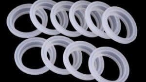
Silicone: Silicone offers excellent flexibility, high-temperature resistance, and superior electrical insulation. Silicone is also non-toxic, making it ideal for medical applications.
Polycarbonate (PC): PC offers high impact resistance and transparency, along with good electrical insulation. It is suitable for protective covers and enclosures in electronics.
Polypropylene (PP): PP is lightweight with good chemical resistance and electrical insulation. It is commonly used in consumer electronics and automotive parts.
Nylon (Polyamide): Nylon is strong, durable, and resistant to wear and chemicals.
Common Design Considerations for PCB Overmolding
Glycerole-Based Silicone (GLS) Viscosity and Quality
Glycerole-Based Silicone (GLS) is a commonly used material in PCB overmolding. During the design phase, two key factors related to GLS must be carefully considered:
The viscosity of GLS is critical for achieving optimal results. If the viscosity is too low, the silicone may bleed into areas of the PCB that require protection, leading to potential damage. Conversely, if the viscosity is too high, it can result in difficulties with filling the mold and extended curing times. Therefore, tuning the viscosity to precise consistency is essential for effective overmolding.
Higher-quality GLS materials exhibit superior electrical insulation and stability under high temperatures. The GLS in the overmolding process must meet quality standards.
Injection Gate Placement
The placement of injection gates is a critical aspect of the PCB overmolding process, as it directly affects the flow of the overmolding material into the mold cavity. The injection gates serve as the entry point for the overmolding material. Their location influences the flow paths, which in turn affects the quality of the final overmold. Incorrect placement can lead to uneven filling, resulting in voids or incomplete encapsulation.
The optimal position for injection gates is typically at the thickest wall section of the mold. This strategic placement helps ensure that the material flows evenly throughout the mold, minimizing the risk of air entrapment and ensuring that there are no voids in the final product.
Machinery Considerations
The machinery used in the PCB overmolding process is also a key consideration.
The machinery must provide the appropriate tonnage and clamping force required to keep the mold closed while the molten resin is injected. The clamping force is essential to prevent the mold from opening under pressure, which could lead to material leakage and defects. When dealing with heavier molds, more tonnage is necessary to ensure that the mold remains securely closed during the injection process. This is particularly important for maintaining the quality of the overmold and ensuring that it adheres properly to the PCB.
How to Prevent PCB Damage During Overmolding?
During the overmolding process, PCBs and sensitive components can be damaged by high temperatures, high pressures, and stress. Here are several methods to prevent PCB damage, covering aspects of design, materials, process, and protection.
Design Optimization
- Balance Thermal Stress: During the design phase, ensure even component placement and trace routing to minimize heat concentration. This reduces the risk of PCB warping and delamination from uneven thermal expansion.
- Control Component Height: Keep component heights to a minimum to reduce the stress applied to protruding parts by the molding material, especially for delicate components.
- Avoid Voltage Gradients: When laying out the board, avoid placing high- and low-voltage pins next to each other. This reduces the risk of electrochemical reactions and corrosion, particularly in humid environments.
- Add Mechanical Support: For critical connectors and components, add mechanical support or use specialized mold designs to distribute stress.
Material Selection
- Choose Low Melting Point Materials: For sensitive components, select overmolding materials with a lower melting point (e.g., certain thermoplastic polyurethanes or silicones) to reduce thermal shock.
- Use High-Quality Substrate: Opt for high-quality substrate materials to prevent delamination and ensure PCB stability during manufacturing.
- Conformal Coating: Apply a conformal coating to the PCB before overmolding. This creates a protective film that resists moisture, contaminants, and chemicals.
- Solder Mask: A high-quality solder mask protects copper traces from oxidation and corrosion.
Process Control
- Precisely Control Parameters: Accurately control the melt temperature, injection speed, and pressure during the injection process. This ensures smooth material flow and prevents excessive force on components.
- Gradual Pressure Application: Increase pressure slowly to minimize mechanical stress.
- Pre-Drying: Before overmolding, pre-dry the PCB to remove internal moisture. Moisture can turn to steam during heating, causing bubbles, cracking, or delamination.
- Use High-Precision Fixtures: Use high-precision fixtures with mechanical guidance or vacuum suction to ensure accurate PCB positioning. This allows for uniform material distribution and prevents functional failure due to misalignment.
- Low-Pressure Molding: For particularly delicate components, use a low-pressure molding process. This method uses lower injection pressures and melt temperatures, applying less stress to the PCB.
Special Protection Measures
- Pre-Encapsulation: For especially sensitive areas, such as sensors, apply a local encapsulation with a soft gel before the main overmolding process for extra protection.
- Accurate Venting Paths: Design venting paths in the mold to allow air to escape smoothly, ensuring uniform material filling.
- Use Cushion Pads: Embed silicone or rubber cushion pads in the mold to protect fragile components from direct pressure.
Reliability Testing
- Perform Reliability Testing: Before mass production, perform thermal cycling, vibration, and stress tests on the overmolded samples. This verifies that the product can withstand expected environmental and mechanical stresses.
Applications of PCB Overmolding
PCB overmolding is widely used across industries to protect circuit boards from moisture, vibration, and mechanical stress while maintaining compact, reliable designs. Typical applications include:
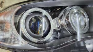
- Automotive Industry: Electronic control units (ECUs), sensors, and connectors
- Consumer Electronics: Smart wearables, earphones, and portable devices
- Industrial Equipment: Controllers, power modules, and communication units
- Lighting Systems: LED driver boards and outdoor lighting modules
- Medical Devices: Diagnostic equipment, monitoring instruments, and wearable devices
- Aerospace and Defense: Control modules, navigation systems, and communication components
Conclusion
PCB overmolding is a powerful manufacturing process that enhances the reliability, durability, and performance of electronic devices. By encapsulating printed circuit boards in a protective layer of plastic or other materials, overmolding service provides a robust barrier against environmental factors such as moisture, dust, and mechanical stress. Don’t hesitate to contact us for assistance with your PCB overmolding projects. Our factory is professional in producing high quality overmolded products and achieving your goals.